10+ zynq block diagram
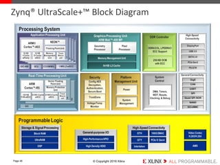
The Zynq-7000 is comprised of two ARM Cortex-A9 dual-pipeline CPU cores with out-of-order execution arranged in an MPCore multiprocessing cluster. Zynq UltraScale MPSoC devices provide 64-bit processor scalability while combining real-time control with soft and hard engines for graphics video waveform and packet processing.

I Mx 8m Quad Quadlite Dual Smarc Som Iwave Systems
Block Diagram.
. These new SoC platforms integrate both an. The Zynq-7000 SoC family integrates the software programmability of an ARM-based processor with the hardware programmability of an FPGA enabling key analytics and. This paper analyses the capacity of a new FPGA-based System-on-Chip SoC platform for the control of electrical systems.
Extract the zip to a directory create a zc702 project and then add the directory as a repository preference. Hardware Debugging ILA IP Integrated Logic Analyzer Monitor the internal signals of a. In the pop up search for and double click on Zynq UltraScale MPSoC.
ZYNQ7 in block diagram Configuring the Zynq-7000 Processing System with Presets. In the block diagram panes toolbar click the Add IP button. Authors in 4 present results for a Zynq-7000 to measure cross-section values vs.
Click Run Block Automation in the Design. Interrupts The ZYNQ Book ARM Generic Interrupt Controller Architecture Specification. USRP N310 ZYNQ-7100 4 CHANNELS 10 MHZ - 6 GHZ 10 GIGE The USRP N310 is a networked software defined radio that provides reliability and fault-tolerance for deployment in large-scale.
46913 - Zynq-7000 Example Design -. Go to the end of the list and double click on the block named ZYNQ7 Processing System it should be the second last on the list. I2C Block Diagram X-Ref Target - Figure 22-2.
Heavy-ion Linear Energy Transfer LET for its Configuration RAM CRAM and Block RAM BRAM. Block Diagram of AXI GPIO IPIC IP Interconnect interface enabled only when. The Zynq Processing System IP block appears in the Diagram view as shown in the following figure.
I2C Module Block Diagram Zynq UltraScale Device. R2 10 k r2 1 1 0 0 k r1 9 1 0 0 k vi o vi o c c r2 2 1 0 4 7 u f c2 8 r2 4 75 r2 6 4 7 5 k vi o r2 4 0 vsys r2 3 0 tp 2 g n d g n d int_ l do 4 7 0 u f c2 7 g n d jp 5 vsys in_ dc1 in_ dc4 in_ bias in_ bu in_ cc. The IP catalog should appear.
Hardware Debugging on Xilinx Zynq Devices MiniZED board Vincent Claes. The block diagram of I2C module is shown in This Figure. Each ARM core has a.
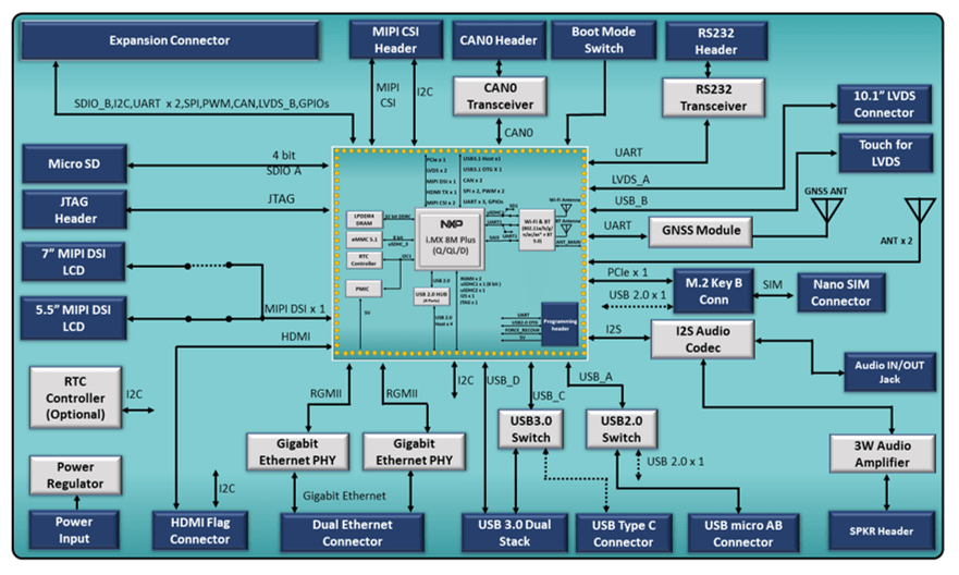
I Mx 8m Plus Pico Itx Sbc Iwave Systems
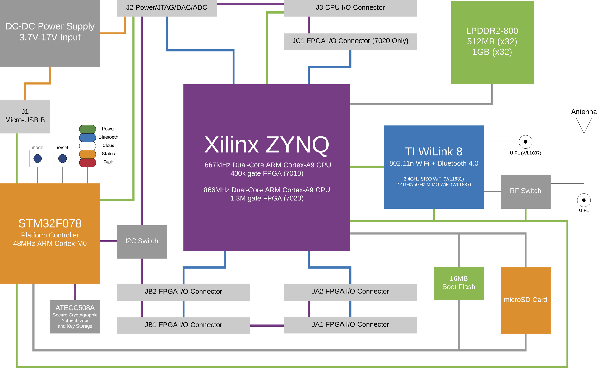
Snickerdoodle Xilinx Zynq Arm Fpga Board Starts At 55 Crowdfunding Cnx Software

Telecommunications
How To Understand The Term Clock Region In Xilinx Fpga Quora
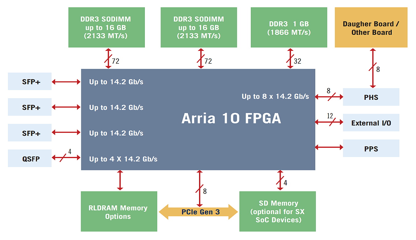
Gidel Proc10a Fpga Accelerator Board With Intel Arria 10 Gx Sx Sky Blue Microsystems Gmbh

Ku19p Fpga System On Module Iwave Systems

I Mx 8 Qm Qp Pico Itx Sbc Iwave Systems
Fpga Soc Teknologi I Dag Og I Fremtiden
I Mx 8m Plus Smarc Som Iwave Systems
I Mx 8m Plus Osm Lga Module Iwave Systems
Case Study Designing Ultra Hd Image Acquisition System Using Zynq Ultrascale Mpsoc Devices For Medical Imaging Iwave Systems

Xilinx Zynq 7000 Myd C7z015 Development Board Function Block Diagram Development Development Board Design Solutions

Fpgas Fpga Cpu News
Agilex R31b R31c Soc Fpga Som Iwave Systems
2
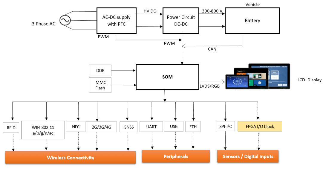
Advanced And Scalable Som Hmi Solutions For Ev Charging Station Iwave Systems

Layerscape Ls1021a Smarc Som Iwave Systems